
The Chip Wave: Complete Chapter-by-Chapter Summary

Welcome to the Precision Silicon Blueprint. Today, we are diving into *The Chip Wave* by Yu Sheng, a definitive look at the forces that built the modern semiconductor supply chain.
This book synthesizes thirty years of technological disruption, business model revolution, and geopolitical tension. It tells the story of how a small island nation transformed itself from a labor exporter into the undisputed king of the world's most critical industry. We are about to explore the blueprint that forged this empire, starting from the very beginning.

The Precision Silicon Blueprint begins with a story that sounds almost too small to change the world: a $10 breakfast in a Taipei soy milk shop. In 1974, Minister Sun Yun-suan and Dr. Pan Wen-yuan sat down with just seven people and a meager budget, yet they made a decision that would pivot an entire economy toward integrated circuits. This moment, known as "The 1974 Breakfast," was the spark that ignited Taiwan's chip revolution.
From that humble start, the strategy evolved into "The RCA Tech Transfer" in 1976. Instead of trying to invent everything from scratch, the state smartly invested $10 million to acquire 7-micron CMOS technology from RCA. This move accelerated the learning curve, allowing Taiwan to catch up with Moore's Law without the risk of starting from zero.
By the 1980s, this momentum culminated in "The Talent Seed." The government created the Industrial Technology Research Institute (ITRI) and the Hsinchu Science Park, effectively building an incubator for the future. By repatriating US-trained engineers and fostering a collaborative ecosystem, Taiwan transformed from a manufacturing hub into a global technology powerhouse. This blueprint didn't just build chips; it built a nation's future.

The slide you're looking at captures the pivotal moment when the semiconductor industry split into two distinct worlds. On the left, you see "The Closed Loop"—the old way. Before 1987, giants like Intel and Texas Instruments were forced to do everything themselves: design the chip and build the factory. It was a high-stakes game where new players couldn't even enter because building a fab cost over $50 million.
But then, in 1987, everything changed. On the right, we see "The Pure-Play Foundry Disruption." Morris Chang founded TSMC with a radical idea: stop designing chips entirely. Instead, focus exclusively on manufacturing for others. By separating chip design from fabrication, TSMC turned the industry from a closed product into an open service. This bold move created a new model where design companies could innovate without the massive burden of building factories, while foundries could scale up production for everyone. This paradigm shift is the foundation of the modern chip ecosystem.

The Precision Silicon Blueprint reveals a fundamental shift in how we build the chips that power our world. On the left, you see the "Old Guard"—the traditional IDM model. Their philosophy is old-school: "Only real men have fabs," as Jerry Sanders famously said. They keep design and manufacturing under one roof, splitting their focus and budget between architecture and physics. This approach creates a monopolistic, guarded ecosystem where capacity is limited by internal sales, making them vulnerable to market cycles.
Contrast that with the "Disruptor" on the right: the pure-play Foundry model. Here, manufacturing is treated as a neutral, pure service platform. Instead of being limited by their own product lines, they pool demand from hundreds of global clients, keeping those capital-intensive machines running 24/7. Their entire R&D budget—100% of it—is dedicated to one thing: shrinking lithographic nodes and optimizing yields. This strategy lowers the barrier to entry dramatically, enabling anyone with a laptop and a CAD file to start a silicon company.
This comparison highlights a pivotal evolution in the industry. While the IDM model has its roots in the era of vertical integration, the Foundry model has democratized innovation, turning chip manufacturing into a scalable, global utility that drives the modern digital economy.

The Precision Silicon Blueprint reveals how TSMC didn't just build a factory—it birthed an entire ecosystem. At the center sits "The Universal Factory," the engine connecting giants like Nvidia, Qualcomm, Broadcom, and Xilinx. Look at Nvidia: in 1995, they couldn't afford their own fab, so they relied on TSMC to manufacture early GPUs, a move that ultimately secured their AI dominance. Similarly, Xilinx pioneered the fabless model, proving that shedding manufacturing baggage accelerates design innovation. Qualcomm focused entirely on CDMA wireless tech, outsourcing mass production of mobile SoCs, while Broadcom and Marvell became telecom disruptors empowered by TSMC's foundry scale. As Professor Michael Porter noted, TSMC didn't just create its own industry; it created its clients' industry. This blueprint shows how one universal factory unlocked the potential for countless innovators to thrive without the burden of manufacturing.
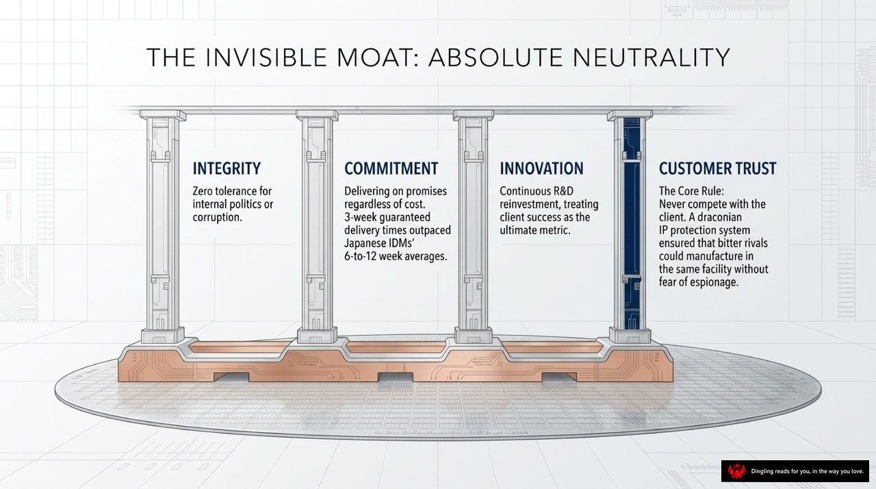
The invisible moat of TSMC isn't just about its factories; it's built on a foundation of absolute neutrality. Look at these four pillars: Integrity, Commitment, Innovation, and Customer Trust. This is the core rule that kept the industry running smoothly.
First, Integrity means zero tolerance for internal politics or corruption. That's the bedrock. Second, Commitment. TSMC delivers on promises regardless of cost. Their 3-week guaranteed delivery times consistently outpaced the 6-to-12 week averages of their Japanese IDM competitors. In a world where speed is everything, that reliability is a superpower.
Then there's Innovation. It's not just about R&D spending; it's about treating client success as the ultimate metric. This philosophy directly feeds into the fourth pillar: Customer Trust. The golden rule here is simple but powerful: Never compete with the client. TSMC implemented a draconian IP protection system, ensuring that even bitter rivals could manufacture in the same facility without any fear of espionage. This unique ability to host competitors side-by-side created an ecosystem where trust became the most valuable currency.
While other foundries struggled with political maneuvering or competing for market share, TSMC chose a different path. By prioritizing the customer's success over their own, they built a fortress that no competitor could breach. This wasn't just a business strategy; it was a cultural shift that defined the entire semiconductor industry for decades.

The immersion lithography miracle is one of the most brilliant pivots in tech history. Back in 2002, the industry hit a hard physical wall at 157 nanometers. Billions of dollars were wasted on dead-end techniques as everyone tried to push light smaller without changing how it worked. But TSMC's Dr. Burn J. Lin saw a different path: adding a 1mm layer of hyper-pure water to refract the light. This simple disruptor changed everything. By using water with a refractive index of 1.44, they effectively reduced the 193nm ArF laser light down to 134nm without needing new, expensive lasers. The result was a $10 billion industry pivot that bypassed the physical wall entirely. This breakthrough crowned ASML as the monopoly of lithography and propelled Moore's Law forward for another decade, proving that sometimes the smartest move isn't to fight the limits, but to cleverly bend the rules around them.

Let's dive into the architecture that saved the chip industry. As we shrink transistors below 20 nanometers, traditional flat gates lose their grip on electron flow, causing a massive leakage crisis that threatens to end Moore's Law. This is the bottleneck we faced in the 2D era.
But here is where the 3D solution changes everything. Enter the FinFET, or 3D transistor. Dr. Hu Chenming's brilliant architecture wraps the gate around a vertical fin, effectively controlling electron flow from three sides instead of just one. This design blocks leakage perfectly and allows us to pack more power into a smaller space.
This shift from planar to 3D didn't just solve a technical glitch; it reignited the semiconductor revolution, allowing us to continue scaling down and pushing the boundaries of what's possible in computing.

Look at this graph titled "The Mobile Divergence." It perfectly captures a pivotal moment in tech history: the moment the world split into two very different paths for computing.
On the left, we see the PC Paradigm, led by Intel. The curve flattens out. Why? Because Intel famously rejected the early iPhone chip contract. They calculated it as unprofitable due to low margins and got stuck in a stagnant PC market. They were tethered to the old world of desktops.
Now, look at the steep climb on the right: The Mobile Paradigm, powered by TSMC. This is where the magic happened. While others hesitated, TSMC embraced mobile SoCs. The strict quality requirements and the massive volume of the iPhone forged an unstoppable alliance with Apple. Apple's sheer scale provided TSMC with billions in guaranteed capital. This funding allowed them to pour money into exorbitant R&D for sub-10nm nodes, creating a self-reinforcing cycle of innovation.
The result is clear on the chart: the mobile path didn't just grow; it exploded. It created a new reality where the constraints of the PC era simply didn't apply anymore. This divergence didn't just change chip manufacturing; it fundamentally reshaped the global economy, proving that the future belonged not to the giants of the past, but to those who could scale for the mobile age.

The Nightingale Project wasn't just about building a factory; it was about orchestrating a total cultural and operational overhaul. Back in 2015, when TSMC lost ground to Samsung's 14nm FinFET, Chairman Morris Chang declared the 10nm node a "must-win battle." The response was immediate and brutal: 400 elite R&D engineers were deployed into a non-stop, 24/7 assembly line, running on a three-shift rotation that never slept. To fuel this relentless pace, the company incentivized its workforce with a +30% base pay hike and +50% bonuses. This extreme work culture didn't just accelerate timelines; it fundamentally shifted the trajectory. TSMC didn't just meet the 10nm target; they crushed the barrier and raced immediately to 7nm, permanently leaving their incumbents behind. While others were still catching up, TSMC had already moved on, proving that in the semiconductor war, speed and operational intensity are the ultimate differentiators.

The slide breaks down the fierce rivalry between the "Silicon Titans," specifically highlighting how TSMC, Samsung, and Intel have diverged in their strategies and current market positions.
Looking at the top section, we see TSMC labeled as the "Pure-Play Hegemon." Their strategy is a clear 100% foundry model, focusing entirely on manufacturing for clients rather than designing chips themselves. This approach has paid off massively, giving them control over more than 53% of the global foundry market and a 90%+ monopoly on advanced nodes like 5nm and 3nm. They are essentially the undisputed leaders in precision silicon blueprints.
In the middle, Samsung is positioned as the "Hybrid Challenger." Unlike TSMC, Samsung plays both sides of the street: they manufacture their own chips while also competing for external foundry clients. While they were the first to announce 3nm GAA technology, the chart indicates they are currently struggling with yield stability and client trust, represented by the caution flags in the graphic.
Finally, at the bottom, we see Intel as the "Fallen Giant." Once a dominant force, Intel's traditional IDM model collapsed at the 14nm node. The "Tick-Tock" strategy failed, leading to significant delays on 10nm and 7nm processes. Consequently, they are now forced to outsource their own advanced CPU manufacturing to external foundries, a stark reversal of their historical dominance.
This visual perfectly captures the shifting landscape of the semiconductor industry: from a time when giants made everything themselves, to a new era where specialized foundries like TSMC hold the keys to the future, while legacy players adapt or fall behind.

Beyond Moore: Advanced Packaging. On the left, you see the traditional monolithic chip—a single, massive piece of silicon. While it once dominated, today it hits a wall. At the 3nm physical limit, manufacturing becomes incredibly expensive with low yields. It's simply too hard to scale.
Look at the right side: Heterogeneous Integration, or Chiplets plus CoWoS. This is the future. Instead of one giant chip, we stack multiple specialized silicon chiplets—GPUs, HBM memory, AI accelerators—horizontally and vertically atop a silicon interposer. This allows us to mix and match best-in-class components, drastically improving performance and bandwidth while cutting costs.
The shift is already happening. As the text notes, CoWoS was once deemed too expensive, but now Nvidia GPUs and Google TPUs rely entirely on it to achieve the massive bandwidth required for artificial intelligence. We are moving from scaling a single die to scaling a system. This isn't just a packaging change; it's the new engine driving the next generation of computing power.

The Digital Bottleneck isn't just a metaphor; it's a massive, real-time crisis shaking the global economy right now. Imagine a funnel where the top is exploding with demand—169 industries, from electric vehicles to medical devices, all screaming for chips. But look at the neck of that funnel: the supply is hyper-concentrated. There is literally only one company on Earth capable of producing advanced 5nm and 3nm chips at scale. This extreme concentration creates a fragile point of failure. When a Texas freeze hits or a factory fire breaks out, the entire system chokes. The result? A global famine. We are seeing auto industries lose over 11 million vehicles simply because they can't find those $1 microcontrollers. This slide illustrates the dangerous reality: we have massive demand flowing into a single, fragile supply line, and the consequences of any disruption are felt by everyone.

The slide we see here captures the brutal reality of today's chip war: Silicon is the new oil, and the map shows all the global power lines converging on East Asia. With over 80% of the world's foundry capacity sitting in that region, the West is facing a genuine choke point. They've poured hundreds of billions into the CHIPS Act and the EU's Digital Compass, trying to build autonomy from scratch. But here's the hard truth the slide highlights: replicating this entire ecosystem is nearly impossible. It's not just about buying machines; it requires decades of unified culture, a massive clustering of hundreds of suppliers, and elite engineering talent working in brutal synchronization. That is the illusion of autonomy. You can't just copy-paste a supply chain; you can't clone the decades of trust and friction that built the original one. While superpowers race to localize, the fundamental advantage remains concentrated where it's been for decades.

The Precision Silicon Blueprint isn't just a title; it's the story of how a single island became the heartbeat of the global digital economy. Look at the text on the screen: in less than fifty years, the pure-play foundry model went from being a ridiculed underdog to the beating heart of the global economy. By severing design from manufacturing, it birthed the fabless ecosystem, rescued Moore's Law from the laws of physics, and crowned a single island as the undisputed epicenter of artificial intelligence and digital survival.
Think about the stakes here. If the digital survival of 169 global industries depends on a microscopic photolithographic canvas sitting atop a single geopolitical fault line, we have to ask ourselves: have we engineered the ultimate triumph of globalization, or its most fragile chokepoint? This slide captures the tension between unprecedented technological dominance and the terrifying fragility of relying on one location for the world's computing power. It's a reminder that while we've built the ultimate machine, the foundation beneath it is thinner than we ever imagined.